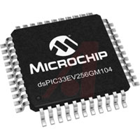
Microchip's dsPIC33EV family of digital signal controllers (DSCs) features a 5 V 70 MIPS dsPIC® DSC core with enhanced on-chip features and is ideal for operating in harsh environments such as appliances and automotive applications. The 5 V dsPIC33EV family comes with rich peripheral integration which includes CAN, SENT, High Speed PWMs, OP Amps and Error Correcting Code Flash for increased reliability and safety. The dsPIC33EV family of devices enable the design of high-performance, precision motor control systems that are more energy efficient. They can be used to control BLDC, permanent magnet synchronous, AC induction and stepper motors. These devices are ideal for automotive applications and high-performance general purpose applications.
Features/Specs:
Operating Conditions:4.5 V to 5.5 V, -40°C to +85°C, DC to 70 MIPS
4.5 V to 5.5 V, -40°C to +125°C, DC to 60 MIPS
4.5 V to 5.5 V, -40°C to +150°C, DC to 40 MIPS
dsPIC33E Core:
Code-Efficient (C and Assembly) Architecture
Two 40-Bit Wide Accumulators
Single-Cycle (MAC/MPY) with Dual Data Fetch
Single-Cycle, Mixed-Sign MUL plus Hardware Divide
32-Bit Multiply Support
Intermediate Security for Memory:
Provides a boot Flash segment in addition to the existing general Flash segment
Error Code Correction (ECC) for Flash
Added Two Alternate Register Sets for Fast Context Switching
High-Speed PWM:
Up to Six Pulse-Width Modulation (PWM) Outputs (three generators)
Primary Master Time Base Inputs allow Time Base Synchronization from Internal/External Sources
Dead Time for Rising and Falling Edges
8.3 ns PWM Resolution at 60 MIPS,
16.6 ns Center-Aligned mode at 60 MIPS
PWM Support for:
DC/DC, AC/DC, inverters, Power Factor Correction (PFC) and lighting
Brushless Direct Current (BLDC), Permanent Magnet Synchronous Motor (PMSM), AC Induction Motor (ACIM), Switched Reluctance Motor (SRM)
Programmable Fault inputs
Flexible trigger configurations for Analog-to-Digital conversion
Independent Time Base
Supports PWM lock, PWM output chopping and dynamic phase shifting
Advanced Analog Features:
ADC module:
Configurable as 10-bit, 1.1 Msps with four S&H or 12-bit, 500 ksps with one S&H
Up to 36 analog inputs
Flexible and Independent ADC Trigger Sources
Up to Four Op Amp/Comparators with Direct Connection to the ADC module
Additional dedicated comparator and 7-bit Digital-to-Analog Converter (DAC)
Programmable references with 128 voltage points
Programmable blanking and filtering
Charge Time Measurement Unit (CTMU):
Supports mTouch™ capacitive touch sensing
Provides high-resolution time measurement (1 ns)
On-chip temperature measurement
Temperature sensor diode
Multiple sources of edge input triggers
Timers/Output Compare/Input Capture:
Nine General Purpose Timers:
Five 16-bit and up to two 32-bit timers/counters, Timer3 can provide ADC trigger
Four Output Capture modules configurable as timers/counters
Four Input Capture modules
Communication Interfaces:
Two Enhanced Addressable UART modules (6.25 Mbps):
Support for LIN/J2602 bus support and IrDA®
High and low speed (SCI)
Two SPI modules (15 Mbps):
25 Mbps data rate without PPS used
One I2C™ module (up to 1 Mbaud) with SMBus Support
Two SENT J2716 (Single Edge Nibble Transmission-Transmit/Receive) module for Automotive Applications
One CAN module
32 buffers, 16 filters and three masks
Direct Memory Access (DMA):
4-Channel DMA with User-Selectable Priority Arbitration
Universal Asynchronous Receiver/Transmitter (UART), Serial Peripheral Interface (SPI), ADC, Input Capture, Output Compare and Controller Area Network (CAN)
Qualification and Class B Support:
AEC-Q100 Rev G (Grade 1: -40°C to +125°C)
AEC-Q100 Rev G (Grade 0: -40°C to +150°C) Planned
DSPIC33EV256GM104-I/ML產(chǎn)品信息


 Datasheet